- 您现在的位置:买卖IC网 > Sheet目录1993 > DS1372U+T&R (Maxim Integrated Products)IC BINARY COUNTER 32-BIT 8-USOP
DS1372
_______________________________________________________________________________________
3
Note 1:
Limits at -40°C are guaranteed by design and not production tested.
Note 2:
All voltages are referenced to ground.
Note 3:
SCL clocking at maximum frequency = 400kHz.
Note 4:
Specified with I2C bus inactive, SCL = SDA = VCC.
Note 5:
Measured with a 32.768kHz crystal attached to the X1 and X2 pins.
Note 6:
The I2C minimum operating frequency is imposed by the requirement of timeout period.
Note 7:
The first clock pulse is generated after this period.
Note 8:
A device must internally provide a hold time of at least 300ns for the SDA signal (referred to as the VIHMIN of the SCL sig-
nal) to bridge the undefined region of the falling edge of SCL.
Note 9:
The maximum tHD:DAT must only be met if the device does not stretch the low period (tLOW) of the SCL signal.
Note 10: A fast-mode device can be used in a standard-mode system, but the requirement tSU:DAT
≥ 250ns must then be met.
This is automatically the case if the device does not stretch the low period of the SCL signal. If such a device does stretch
the low period of the SCL signal, it must output the next data bit to the SDA line tR(MAX) + tSU:DAT = 1000 + 250 = 1250ns
before the SCL line is released.
Note 11: CB = Total capacitance of one bus line in pF.
Note 12: The parameter tOSF is the period of time the oscillator must be stopped for the OSF flag to be set over the voltage range of
2.4V
≤ VCC ≤ VCC(MAX).
Note 13: The DS1372 can detect any single SCL clock held low longer than T_TIMEOUT (MIN). The I2C interface is in reset state and
can receive a new START condition when SCL is held low for at least T_TIMEOUT (MAX). Once the part detects this condi-
tion the SDA output is released. The oscillator must be running for this function to work.
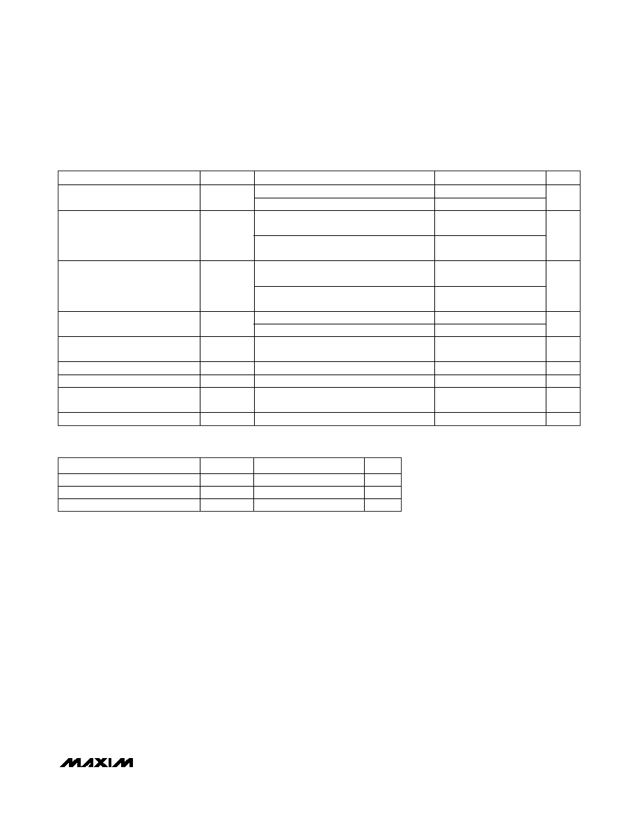
ELECTRICAL CHARACTERISTICS (continued)
(VCC = 2.4V to 5.5V, TA = -40°C to +85°C, unless otherwise noted.) (Note 1)
PARAMETER
SYMBOL
CONDITIONS
MIN
TYP
MAX
UNITS
Fast mode
100
Data Setup Time (Note 10)
tSU:DAT
Standard mode
250
ns
Fast mode
20 +
0.1CB
300
Rise Time of SDA and SCL
Signals (Note 11)
tR
Standard mode
20 +
0.1CB
1000
ns
Fast mode
20 +
0.1CB
300
Fall Time of SDA and SCL Signals
(Note 11)
tF
Standard mode
20 +
0.1CB
300
ns
Fast mode
0.6
Setup Time for STOP Condition
tSU:STO
Standard mode
4.0
μs
Capacitive Load for Each Bus
Line (Note 11)
CB
400
pF
I/O Capacitance
CI/O
10
pF
SCL Spike Suppresion
TSP
30
ns
Oscillator Stop Flag (OSF) Delay
(Note 12)
tOSF
100
ms
Timeout Interval (Note 13)
T_TIMEOUT
25
35
ms
CRYSTAL SPECIFICATIONS
PARAMETER
SYMBOL
MIN
TYP
MAX
UNITS
Nominal Frequency
fO
32.768
kHz
Capacitive Load
CL
12.5
pF
Equivalent Series Resistance
ESR
50
k
I2C, 32-Bit, Binary Counter Clock with 64-Bit ID
发布紧急采购,3分钟左右您将得到回复。
相关PDF资料
DS1374C-3#
IC RTC I2C W/CHARGER 16-SOIC
DS1375T+
IC RTC SERIAL W/ALARM 6-TDFN
DS1384FP-12+
IC CTRLR RTC WDOG 120NS 44-MQFP
DS1386P-8-120+
IC TIMEKEEPER RAM 64K 34-PCM
DS1388Z-3+T&R
IC RTC I2C W/CHARGER 8-SOIC
DS1391U-3+
IC RTC W/CHARGER 10-USOP
DS1394U-33+T&R
IC RTC SPI 3WIRE W/CHRGR 10-MSOP
DS14285SN+T&R
IC RTC W/NV RAM CNTRL 24-SOIC
相关代理商/技术参数
DS1374
制造商:MAXIM 制造商全称:Maxim Integrated Products 功能描述:I2C, 32-Bit Binary Counter Watchdog RTC with Trickle Charger and Reset Input/Output
DS1374_10
制造商:MAXIM 制造商全称:Maxim Integrated Products 功能描述:I2C, 32-Bit Binary Counter Watchdog RTC with Trickle Charger and Reset Input/Output
DS1374C-18
功能描述:实时时钟 I2C 32-Bit Binary Counter Watchdog RoHS:否 制造商:Microchip Technology 功能:Clock, Calendar. Alarm RTC 总线接口:I2C 日期格式:DW:DM:M:Y 时间格式:HH:MM:SS RTC 存储容量:64 B 电源电压-最大:5.5 V 电源电压-最小:1.8 V 最大工作温度:+ 85 C 最小工作温度: 安装风格:Through Hole 封装 / 箱体:PDIP-8 封装:Tube
DS1374C-18-
制造商:MAXIM 制造商全称:Maxim Integrated Products 功能描述:I2C, 32-Bit Binary Counter Watchdog RTC with Trickle Charger and Reset Input/Output
DS1374C-18#
功能描述:实时时钟 I2C 32-Bit Binary Counter Watchdog RoHS:否 制造商:Microchip Technology 功能:Clock, Calendar. Alarm RTC 总线接口:I2C 日期格式:DW:DM:M:Y 时间格式:HH:MM:SS RTC 存储容量:64 B 电源电压-最大:5.5 V 电源电压-最小:1.8 V 最大工作温度:+ 85 C 最小工作温度: 安装风格:Through Hole 封装 / 箱体:PDIP-8 封装:Tube
DS1374C-3
功能描述:实时时钟 I2C 32-Bit Binary Counter Watchdog RoHS:否 制造商:Microchip Technology 功能:Clock, Calendar. Alarm RTC 总线接口:I2C 日期格式:DW:DM:M:Y 时间格式:HH:MM:SS RTC 存储容量:64 B 电源电压-最大:5.5 V 电源电压-最小:1.8 V 最大工作温度:+ 85 C 最小工作温度: 安装风格:Through Hole 封装 / 箱体:PDIP-8 封装:Tube
DS1374C-3-
制造商:MAXIM 制造商全称:Maxim Integrated Products 功能描述:I2C, 32-Bit Binary Counter Watchdog RTC with Trickle Charger and Reset Input/Output
DS1374C-3#
功能描述:实时时钟 I2C 32-Bit Binary Counter Watchdog RoHS:否 制造商:Microchip Technology 功能:Clock, Calendar. Alarm RTC 总线接口:I2C 日期格式:DW:DM:M:Y 时间格式:HH:MM:SS RTC 存储容量:64 B 电源电压-最大:5.5 V 电源电压-最小:1.8 V 最大工作温度:+ 85 C 最小工作温度: 安装风格:Through Hole 封装 / 箱体:PDIP-8 封装:Tube